A thin device triggers one of quantum mechanics’ strangest and most useful phenomena

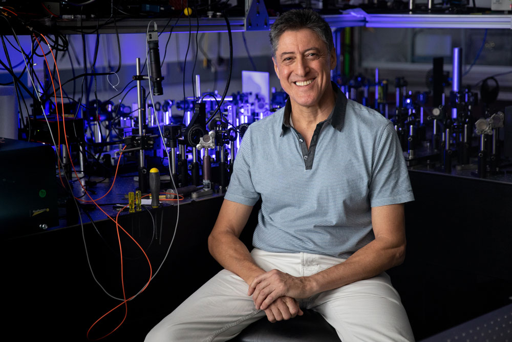
(Photo by Craig Fritz)
An ultrathin invention could make future computing, sensing and encryption technologies remarkably smaller and more powerful by helping scientists control a strange but useful phenomenon of quantum mechanics, according to new research recently published in the journal Science.
Scientists at Sandia and the Max Planck Institute for the Science of Light have reported on a device that could replace a roomful of equipment to link photons in a bizarre quantum effect called entanglement. This device — a kind of nano-engineered material called a metasurface — paves the way for entangling photons in complex ways that have not been possible with compact technologies.
When scientists say photons are entangled, they mean they are linked in such a way that actions on one affect the other, no matter where or how far apart the photons are in the universe. It is an effect of quantum mechanics, the laws of physics that govern particles and other very tiny things.
Although the phenomenon might seem odd, scientists have harnessed it to process information in new ways. For example, entanglement helps protect delicate quantum information and correct errors in quantum computing, a field that could someday have sweeping impacts in areas such as national security, science and finance. Entanglement is also enabling new, advanced encryption methods for secure communication.
Research for the groundbreaking device, which is a hundred times thinner than a sheet of paper, was performed, in part, at the Center for Integrated Nanotechnologies, a DOE Office of Science user facility operated by Sandia and Los Alamos national laboratories. Sandia’s team received funding from the Office of Science, Basic Energy Sciences program.
Light goes in, entangled photons come out
The new metasurface acts as a doorway to this unusual quantum phenomenon. In some ways, it’s like the mirror in Lewis Carroll’s “Through the Looking-Glass,” through which the young protagonist Alice experiences a strange, new world.
Instead of walking through their new device, scientists shine a laser through it. The beam of light passes through an ultrathin sample of glass covered in nanoscale structures made of a common semiconductor material called gallium arsenide.

“It scrambles all the optical fields,” said Sandia senior scientist Igal Brener, an expert in a field called nonlinear optics who led the Sandia team. Occasionally, he said, a pair of entangled photons at different wavelengths emerge from the sample in the same direction as the incoming laser beam.
Igal said he is excited about this device because it is designed to produce complex webs of entangled photons — not just one pair at a time, but several pairs all entangled together, and some that can be indistinguishable from each other. Some technologies need these complex varieties of so-called multi-entanglement for sophisticated information processing schemes.
Other miniature technologies based on silicon photonics can also entangle photons but without the much-needed level of complex multi-entanglement. Until now, the only way to produce such results was with multiple tables full of lasers, specialized crystals and other optical equipment.
“It is quite complicated and kind of intractable when this multi-entanglement needs more than two or three pairs,” Igal said. “These nonlinear metasurfaces essentially achieve this task in one sample when before it would have required incredibly complex optical setups.”
The Science paper outlines how the team successfully tuned their metasurface to produce entangled photons with varying wavelengths, a critical precursor to generating several pairs of intricately entangled photons simultaneously.
However, the researchers note in their paper that the efficiency of their device — the rate at which they can generate groups of entangled photons — is lower than that of other techniques and needs to be improved.
What is a metasurface?
A metasurface is a synthetic material that interacts with light and other electromagnetic waves in ways conventional materials can’t. Commercial industries, said Igal, are busy developing metasurfaces because they take up less space and can do more with light than, for instance, a traditional lens.
“You now can replace lenses and thick optical elements with metasurfaces,” Igal said. “Those types of metasurfaces will revolutionize consumer products.”
Sandia is one of the leading institutions in the world performing research in metasurfaces and metamaterials. Between its Microsystems Engineering, Science and Applications complex, which manufactures compound semiconductors, and the nearby Center for Integrated Nanotechnologies, researchers have access to all the specialized tools they need to design, fabricate and analyze these ambitious new materials.

“The work was challenging as it required precise nanofabrication technology to obtain the sharp, narrowband optical resonances that seeds the quantum process of the work,” said Sylvain Gennaro, a former postdoctoral researcher at Sandia who worked on several aspects of the project.
The device was designed, fabricated and tested through a partnership between Sandia and a research group led by physicist Maria Chekhova, an expert in the quantum entanglement of photons at the Max Planck Institute for the Science of Light.
“Metasurfaces are leading to a paradigm shift in quantum optics, combining ultrasmall sources of quantum light with far-reaching possibilities for quantum state engineering,” said Tomás Santiago-Cruz, a member of the Max Planck team and first author on the paper.
Igal, who has studied metamaterials for more than a decade, said this newest research could possibly spark a second revolution — one that sees these materials developed not just as a new kind of lens, but as a technology for quantum information processing and other new applications.
“There was one wave with metasurfaces that is already well established and on its way. Maybe there is a second wave of innovative applications coming,” he said.