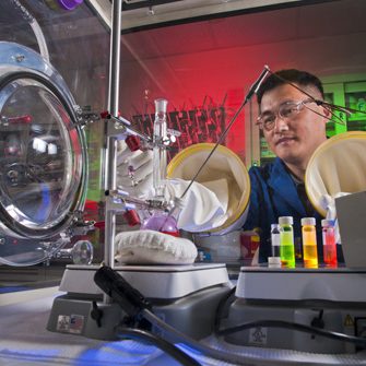
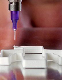
Sandia is home to the Advanced Materials Laboratory (AML), a state-of-art facility that spans the full range of AM from creating custom-engineered AM materials with unique properties, to process and equipment R&D, to prototype hardware manufacture and testing. The AML has a variety of direct-write and laser printing platforms together with scalable sheet-to-sheet printing and coating tools that compliment laser and direct write platforms. Gravure (intaglio printing) and flexographic (relief) printing methods available with tools, such as the Superproofer shown here, allow for high-throughput (printing many devices), wide-areas (10s of square inches), several registered layers, and small features (down to 2 microns, significantly smaller than direct write methods).

Scalable multi-material applications
At the AML, emphasis is on scalable multi-material applications, such as printed electronics and multi-component hardware. Materials and process R&D are tightly integrated with functional prototyping and testing. AML researchers can turn nearly any chemical element into a functional, printable ink. The intended function of the printed part dictates the type of ink and constituent materials; i.e., printed electronics and photonics may require conductive, dielectric, photoluminescent, and semi-conductor materials. Materials can also be integrated to impart trust and security features into printed parts.


